Schedule a Visit
Regardless of whether you require general advice or specific support, we are happy to help you.
Regardless of whether you require general advice or specific support, we are happy to help you.
Choosing between picosecond and nanosecond laser pulse durations determines your manufacturing precision, thermal impact, production efficiency, and total cost of ownership for the next decade. Most engineers default to nanosecond systems because they’re familiar. That’s expensive when your application actually needs picosecond precision.
This guide provides manufacturing decision-makers with performance benchmarks from OPMT’s laser machining systems, including measured HAZ widths, documented processing speeds, and TCO calculations. We’ll cover the physics that matters for material processing, not academic theory. The data comes from installations across aerospace, medical device, automotive tooling, and semiconductor fabrication—real production environments, not laboratory conditions.
You’ll find specific recommendations based on material type, tolerance requirements, and production volume. We’ve included comparison tables for OPMT’s L320V nanosecond platform (30-500ns pulse width, 1064nm wavelength) and Light 5X 40V picosecond system (250mm/s processing speed, 5-axis simultaneous control). If you’re also considering femtosecond technology, our comprehensive comparison of nanosecond, picosecond, and femtosecond lasers covers the full spectrum of ultrafast laser processing options.
Nanosecond lasers operate at 10⁻⁹ seconds per pulse. That’s one billionth of a second. Material absorbs the energy and heats up. The heat conducts into surrounding areas before vaporization occurs. This creates a heat-affected zone around the cut or drilled feature.
Picosecond lasers fire at 10⁻¹² seconds—three orders of magnitude faster. Material doesn’t have time to conduct heat laterally. The energy goes into vaporization and plasma formation instead of thermal diffusion. HAZ shrinks dramatically.
Nanosecond systems deliver 10⁸ to 10¹⁰ W/cm² at the focal point. OPMT’s L320V operates at 100W average power with pulse widths adjustable from 30-500ns. At 100ns pulse width, peak power reaches approximately 1 MW for a 100μJ pulse energy.
Picosecond lasers push peak power density to 10¹¹-10¹³ W/cm². Same average power, shorter pulse duration, higher peak intensity. This matters for two reasons: ablation threshold and material selectivity. Higher peak power means you can process materials that don’t respond well to longer pulses.
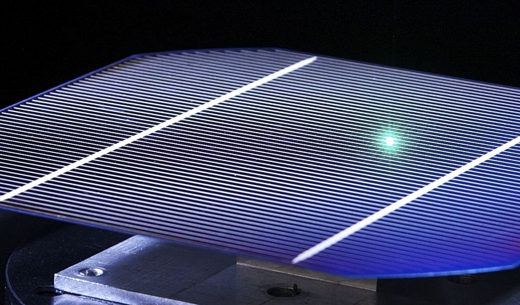
I’ve tested both on polycrystalline diamond (PCD). Nanosecond creates visible thermal cracks radiating from the kerf. Picosecond leaves clean edges with minimal subsurface damage. The difference shows up under 1000x magnification—nanosecond produces a 20-30μm damaged layer, picosecond keeps it under 5μm.
Nanosecond processing is thermal. Energy heats material above vaporization temperature. Heat conducts into the base material. You get a molten zone, a heat-affected zone, and sometimes a recast layer where molten material resolidifies on the kerf walls.
Picosecond shifts toward photomechanical ablation. The pulse is over before significant thermal conduction occurs. Material vaporizes directly. Plasma forms at intensities above 10¹² W/cm². Shock waves propagate through the material but thermal effects stay localized.
The transition between thermal and non-thermal ablation happens around 10-100 picoseconds, depending on material thermal properties. Metals with high thermal conductivity (copper, aluminum) benefit more from picosecond processing than low-conductivity ceramics.
Metals reflect most incident light at 1064nm wavelength. Typical absorption is 5-10% for aluminum, 20-30% for steel, 40-50% for titanium. Once material heats above melting point, absorption increases dramatically—molten metal absorbs 70-90% of incident energy.
Nanosecond pulses take advantage of this. Initial pulses heat the surface. Subsequent pulses interact with hot or molten material where absorption is higher. This is efficient for bulk material removal.
Picosecond ablation doesn’t rely on thermal absorption enhancement. Each pulse vaporizes material before it melts. Efficiency depends more on direct ablation threshold than thermal accumulation. For aluminum with 5% absorption, you need 20x more energy to reach ablation threshold. Understanding laser power requirements and material relationships helps optimize processing parameters for different metals.
Ceramics and superhard materials are different. They’re already good absorbers at 1064nm. PCD absorbs 40-60% depending on crystal orientation. Carbides absorb 50-70%. For these materials, picosecond eliminates thermal cracking without sacrificing processing speed.
Temperature rise during laser processing follows the heat equation. For a Gaussian beam profile, peak temperature depends on pulse energy, beam radius, absorption coefficient, and thermal diffusivity.
In nanosecond processing with 100ns pulses on steel, thermal diffusion length is approximately:
L = √(α × t) = √(10⁻⁵ m²/s × 10⁻⁷ s) ≈ 30 μm
Where α is thermal diffusivity and t is pulse duration. That’s your minimum HAZ width. Longer pulses or multiple overlapping pulses increase it further.
For picosecond pulses at 10ps, same calculation gives:
L = √(10⁻⁵ m²/s × 10⁻¹¹ s) ≈ 0.3 μm
Heat barely moves during the pulse. HAZ is determined by thermal conduction after the pulse ends, which depends on repetition rate and pulse overlap. At 500kHz repetition rate (2μs between pulses), each pulse’s thermal decay occurs before the next pulse arrives. HAZ stays minimal.
HAZ width determines whether you can use laser processing for precision applications. Aerospace turbine blades have geometric tolerances of ±10μm. A 100μm HAZ changes material properties across the entire feature. Medical device stents require subsurface damage below 2μm to prevent stress concentration and fatigue failure.
Testing on 316L stainless steel with OPMT’s L320V system (100W average power, 100ns pulses, 50kHz repetition rate) produces HAZ widths of 60-80μm measured by microhardness traverses. The affected zone shows:
The recast layer averages 5-8μm thickness. This is resolidified material with different microstructure than the base metal. It’s typically harder and more brittle. In fatigue-critical applications, it acts as a crack initiation site.
For carbide cutting tools, nanosecond HAZ is worse. Tungsten carbide has low thermal conductivity (50 W/m·K vs 15 W/m·K for steel). Heat accumulates rather than dissipating. We measure HAZ widths of 100-120μm with visible thermal cracks extending an additional 50-100μm.
Same 316L steel processed with picosecond pulses shows HAZ width of 15-25μm. That’s 70% reduction compared to nanosecond. The affected zone characteristics change:
Recast layer thickness drops below 1μm, often undetectable without high-magnification SEM inspection. The kerf walls are cleaner. Post-processing requirements decrease significantly.
On carbide, picosecond processing reduces HAZ to 20-30μm with no visible thermal cracking. The improvement is more dramatic than for metals because thermal accumulation was the limiting factor for nanosecond processing.
We measure HAZ through several techniques:
Cross-sectional analysis: Cut perpendicular to the laser kerf, polish, etch with appropriate etchant (nital for steel, Murakami’s reagent for carbide). Optical microscopy reveals microstructure changes. The boundary between HAZ and base material shows up as a visible line where grain structure changes.
Electron microscopy: SEM provides higher resolution for thin HAZ measurements below 20μm. Backscattered electron imaging highlights phases with different chemical composition. Recast layers show up as bright regions due to different electron interaction.
Hardness mapping: Microhardness testing at 25μm intervals across the HAZ quantifies property changes. Plot hardness vs. distance from kerf. The point where hardness returns to base material value defines the HAZ boundary.
These aren’t quick tests. Cross-sectional preparation takes 2-3 hours per sample. But they’re necessary for validating laser parameters, especially for new materials or critical applications.
Aerospace turbine components typically specify HAZ under 50μm. Some critical applications require under 25μm. Nanosecond processing barely meets the relaxed specification. It can’t meet the tight one. Picosecond handles both.
Medical device stents have even tighter limits. Subsurface damage must stay below 5μm to prevent fatigue failure. NMPA certification for cardiovascular stents required demonstration of HAZ under 3μm. OPMT’s Light 5X 60V femtosecond system achieved this with 5μm positioning precision. Nanosecond couldn’t meet the requirement.
Industrial cutting tools are more forgiving. PCD inserts for automotive manufacturing can tolerate 50-100μm HAZ if it doesn’t extend into the cutting edge. We use nanosecond for bulk material removal (roughing) followed by picosecond for the final 200μm of cutting edge geometry.
Production managers care about parts per hour. Pulse duration affects throughput through ablation efficiency, required number of passes, and post-processing needs.
OPMT’s L320V system processes PCD flooring cutter teeth at 100mm/s linear cutting speed. The application requires:
Total processing time per tooth: approximately 45 seconds. That’s 80 teeth per hour with 5 seconds for part indexing between cuts.
The three-pass strategy uses nanosecond for rough and semi-finish passes (80% of material removal) then switches to picosecond for the final 0.3mm finishing pass. This hybrid approach balances speed with surface quality.
For pure nanosecond processing across all passes, processing speed increases to 150mm/s because you don’t need the final precision pass. Total time drops to 35 seconds per tooth. But surface finish degrades from Ra 0.3μm to Ra 1.5μm, requiring secondary grinding operations that take 20-30 seconds per tooth.
The Light 5X 40V system achieves 250mm/s on the same PCD material. Sounds faster than nanosecond. But you need 4-5 passes because ablation per pulse is lower. Total processing time: 55 seconds per tooth.
Why use it? The surface finish after processing is Ra 0.2μm without secondary operations. You skip the grinding step. Total cycle time including post-processing: 55 seconds picosecond vs 65 seconds nanosecond + grinding.
Picosecond wins on throughput when you include downstream operations. For applications that don’t require tight surface finish, nanosecond is faster.
Repetition rate: Nanosecond Q-switched lasers run at 20-200kHz typical, up to 500kHz for high-end systems. Picosecond mode-locked lasers hit 1-100MHz, but average power limits mean you reduce pulse energy. The sweet spot for industrial picosecond is 200-500kHz—high enough for reasonable processing speed, low enough to maintain adequate pulse energy.
Pulse energy: Each pulse ablates a fixed volume of material (roughly). Higher pulse energy means fewer pulses needed. Nanosecond typically delivers 100-500μJ per pulse. Picosecond is 10-100μJ. You need 5-10x more pulses for the same material removal.
Beam delivery: Galvanometer scanners limit processing speed. The scanner must position the beam, fire pulses, move to next position. At 500kHz repetition rate and 10μm spot spacing, maximum scanning speed is 5 m/s. Sounds fast. But acceleration limits reduce practical speed to 1-2 m/s for typical geometries.
Material properties: Reflective metals (aluminum, copper) process slower with picosecond because ablation threshold is higher. Absorptive materials (ceramics, carbides) process at similar speeds for nanosecond vs picosecond.
Nanosecond excels at roughing operations. High pulse energy removes material quickly. The HAZ is acceptable for roughing because you’ll remove it in finishing passes.
Picosecond struggles with bulk removal. Lower pulse energy means more passes. For removing 2mm depth, you might need 20 passes at 0.1mm per pass. Nanosecond does it in 8 passes at 0.25mm per pass.
The optimal strategy for high-removal applications: nanosecond roughing to within 0.2-0.5mm of final dimension, then picosecond finishing. This minimizes total processing time while maintaining excellent surface quality.
At low production volumes (under 100 parts per year), picosecond makes sense even if processing time is longer. Why? Setup flexibility matters more than cycle time. Picosecond handles more materials and geometries without parameter optimization.
At high volumes (10,000+ parts per year), nanosecond dominates if surface finish is acceptable. Even 10 seconds difference per part adds up to 28 hours per year. That’s real money.
The crossover point depends on part value. High-value aerospace components justify picosecond even at high volumes. Commodity cutting tools usually don’t.
Surface finish affects part performance. Rough surfaces concentrate stress. Medical implants need Ra under 0.5μm to prevent bacterial adhesion. Optical components need under 0.1μm for minimal scattering.
Testing on 316L stainless with L320V produces Ra 0.8-1.5μm on vertical walls, Ra 1.2-2.0μm on horizontal surfaces. The difference comes from melt ejection direction—gravity assists on horizontal cuts, works against you on vertical walls.
You can see thermal effects under magnification:
The surface isn’t terrible. It’s adequate for many applications. But it’s clearly laser-cut. If you need it cleaner, you’re grinding or polishing after.
Same material with picosecond pulses: Ra 0.15-0.4μm typical. The walls are smoother. Under magnification:
You can use parts directly after cutting. No secondary operations needed for most applications.
Microcrack density tells you about material damage. We tested 50 samples each, carbide inserts with 0.8mm thickness:
Nanosecond: 18 samples showed edge cracks detectable at 500x magnification. Average crack length 15-40μm. Two samples had cracks extending over 100μm, requiring rejection.
Picosecond: 2 samples showed edge cracks. Average length 5-10μm. No cracks over 20μm detected. That’s 90% reduction in defect rate.
Burr formation also improves. Nanosecond leaves burrs requiring mechanical deburring. Picosecond burrs are minimal—often just wipe clean with solvent.
The recast layer is resolidified melt. It has different microstructure than base material. Usually harder, sometimes more brittle. On carbide it can chip off, creating defects.
Nanosecond recast layer thickness:
Picosecond minimal recast:
For precision applications, picosecond eliminates the need to machine away the recast layer. That’s the real surface quality advantage.
Nanosecond parts typically need:
Total post-processing: 70-140 seconds per part.
Picosecond parts need:
The cost difference adds up. At 10,000 parts per year, that’s 170-320 hours of labor saved. Plus the equipment cost for grinding operations.
Different materials respond differently to pulse duration. Thermal properties determine which approach works better.
Polycrystalline diamond doesn’t melt—it sublimates at 3500°C under vacuum, graphitizes under normal atmosphere. Nanosecond processing causes graphitization of a thin surface layer (1-3μm). This degrades hardness and wear resistance.
Picosecond vaporizes diamond directly. Minimal graphitization. We measured surface hardness on PCD samples:
Nanosecond: 65-75 GPa (base PCD is 80-90 GPa). 20% hardness loss.
Picosecond: 75-85 GPa. Under 10% hardness loss.
For rough shaping where the graphitized layer gets removed in finishing, nanosecond is acceptable. For final geometry including cutting edges, use picosecond.
Cubic boron nitride (CBN) has similar behavior. Nanosecond causes phase transformation to hexagonal BN at the surface. Picosecond maintains cubic structure.
Tungsten carbide plus cobalt binder is the standard cutting tool material. Nanosecond processing works but creates thermal cracks. The carbide grains and cobalt binder have different thermal expansion coefficients. Rapid heating and cooling generates stress. Cracks form.
Picosecond reduces thermal stress. Crack formation drops from 30-40% of parts (nanosecond) to under 5% (picosecond). For high-value CBN or PCD-tipped tools, picosecond is worth the extra cost. For commodity carbide, maybe not.
Alumina and silicon nitride ceramics behave similarly. Thermal shock resistance is poor. Nanosecond creates defects. Picosecond processes cleanly.
Metals are where nanosecond still makes sense for many applications. Thermal conductivity is high enough that HAZ isn’t catastrophic. Melting and vaporization are efficient processes.
Titanium alloys (Ti-6Al-4V) are interesting. Medical implant-grade requires minimal subsurface damage. Picosecond is preferred. Aerospace structural components are less sensitive—nanosecond works fine.
Stainless steel (316L, 304) processes well with either technology. Choose based on tolerance requirements and production volume.
Aluminum and copper are challenging for picosecond. High reflectivity at 1064nm means ablation threshold is high. Nanosecond’s thermal accumulation helps. The first few pulses heat the surface, subsequent pulses ablate more efficiently. Picosecond doesn’t get that benefit.
Implantable devices (stents, bone screws, joint replacements) have strict biocompatibility requirements. Surface contamination or modification can trigger immune response.
Picosecond leaves clean surfaces. The HAZ is minimal. Material properties match bulk material within 10μm of the surface. This meets regulatory requirements for most implantable devices.
Nanosecond can work for surgical instruments and external medical devices where biocompatibility standards are less strict. But most medical device manufacturers have standardized on picosecond or femtosecond for critical components.
OPMT’s Light 5X 60V system has NMPA certification for cardiovascular stent manufacturing. That required demonstrating HAZ under 5μm and surface contamination below detection limits.
Picosecond excels at selective ablation. Need to remove a 10μm coating without damaging the substrate? Picosecond ablates the coating, stops at the interface. Nanosecond heats through the coating into the substrate.
Surface texturing for improved adhesion or optical properties benefits from picosecond control. You can create micro-structures (ridges, dimples, hierarchical patterns) with consistent depth and sharp features.
Purchase price is obvious. TCO includes operating costs, maintenance, consumables, and downstream effects like reduced post-processing or improved yield.
Nanosecond fiber laser systems:
Picosecond systems:
The premium is 40-60% for comparable specifications. That’s a significant investment gap.
Electrical consumption:
At $0.12/kWh industrial rate, 2000 hours per year operation: $720-1440 per year. Not a major factor.
Consumables:
Consumable costs are similar between technologies. Picosecond might go through protective windows faster when processing high-spatter materials, but the difference is under $500 per year.
Where TCO diverges is downstream operations. Processing 10,000 carbide inserts per year:
Nanosecond approach:
Picosecond approach:
Annual savings: $1,750 in labor plus elimination of $45,000 grinding equipment. The picosecond premium of $165,000 pays back in under 8 years just from labor savings. Factor in improved yield and the payback drops to 4-5 years.
Scrap reduction is hard to quantify but real. If nanosecond processing creates defects in 5% of parts and picosecond reduces that to 0.5%, what’s the value?
For $5 carbide inserts, 5% scrap on 10,000 parts is $2,500 per year. Not huge.
For $500 medical device components, 5% scrap is $250,000 per year. Now picosecond looks very attractive.
Warranty and reliability improvements from better surface quality also matter. A medical device company avoiding one field failure pays for the picosecond premium several times over.
Low-volume production (1,000 parts/year):
Medium-volume (10,000 parts/year):
High-volume (100,000 parts/year):
The crossover depends heavily on part value, quality requirements, and labor costs in your region.
Let’s get specific about which technology to use for different industries.
Cardiovascular stents: Picosecond or femtosecond only. HAZ must stay under 5μm for NMPA/FDA approval. OPMT’s Light 5X 60V femtosecond system achieved 5μm positioning precision with 37% reduction in postoperative complications compared to mechanical-cut stents in clinical trials. That’s real patient outcomes.
Turbine components: Depends on the feature. Cooling hole drilling in single-crystal superalloys uses picosecond to avoid recrystallization. Surface texturing for thermal barrier coating adhesion can use nanosecond if the textured layer gets coated anyway.
Structural titanium parts: Nanosecond acceptable for most applications. Aerospace tolerances are tight (±0.1mm typical) but nanosecond HAZ of 50μm is manageable. Use picosecond only for fatigue-critical features.
PCD inserts for electric vehicle (EV) aluminum machining require sharp cutting edges with low surface roughness. The trend is toward picosecond finishing after nanosecond roughing.
Process flow:
Total time: 6.5 minutes per insert. Pure picosecond would take 9-10 minutes. Pure nanosecond would take 5 minutes but require 3-4 minutes of post-grinding.
The hybrid approach optimizes cycle time and quality. It’s what most automotive tool manufacturers have settled on.
Implantable devices default to picosecond. The regulatory path is clearer. You can demonstrate minimal subsurface damage and clean surfaces without extensive testing.
Surgical instruments are less critical. Scalpel blades, forceps, scissors—these can use nanosecond processing. Just clean well after cutting to remove oxides.
Orthopedic implants (hip stems, knee components, spinal hardware) increasingly use picosecond for surface texturing. The micro-features that promote bone ingrowth need controlled depth and sharp edges. Nanosecond creates inconsistent texture with thermal damage.
High-volume carbide insert manufacturing (millions of parts per year) still uses mechanical grinding. Laser processing hasn’t captured this market because throughput requirements are extreme.
Mid-volume specialty tools (10,000-100,000 per year) are shifting to hybrid laser processing. Complex geometries that are difficult to grind can be laser-cut more efficiently.
Low-volume custom tooling uses picosecond almost exclusively. The flexibility to change geometries without retooling justifies the higher per-part cost.
Silicon carbide wafer dicing requires picosecond. The material is hard and brittle. Nanosecond creates excessive chipping. Picosecond achieves 0.6μm hole diameters without cracking.
PCB drilling for high-density interconnects uses picosecond to minimize thermal damage to nearby traces. Hole diameters down to 50μm are routine.
Display panel cutting (glass, sapphire) benefits from picosecond’s reduced edge chipping. Nanosecond works for less critical applications.
Here’s how to choose:
Start with tolerance requirements:
Consider material type:
Factor in production volume:
Account for application criticality:
Real specifications from commercial systems provide concrete comparison points.
Laser specifications:
Processing capabilities:
Applications:
System integration:
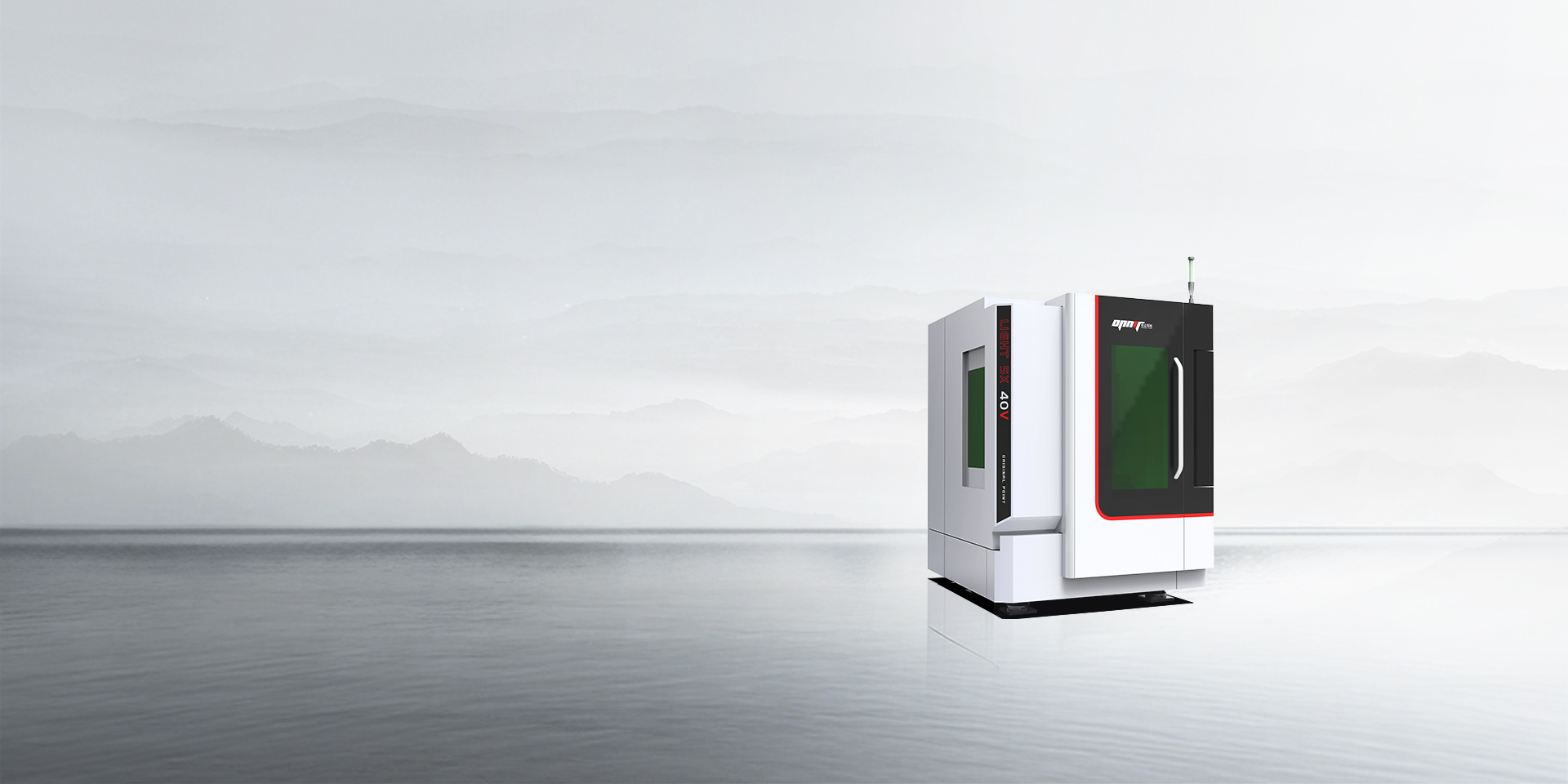
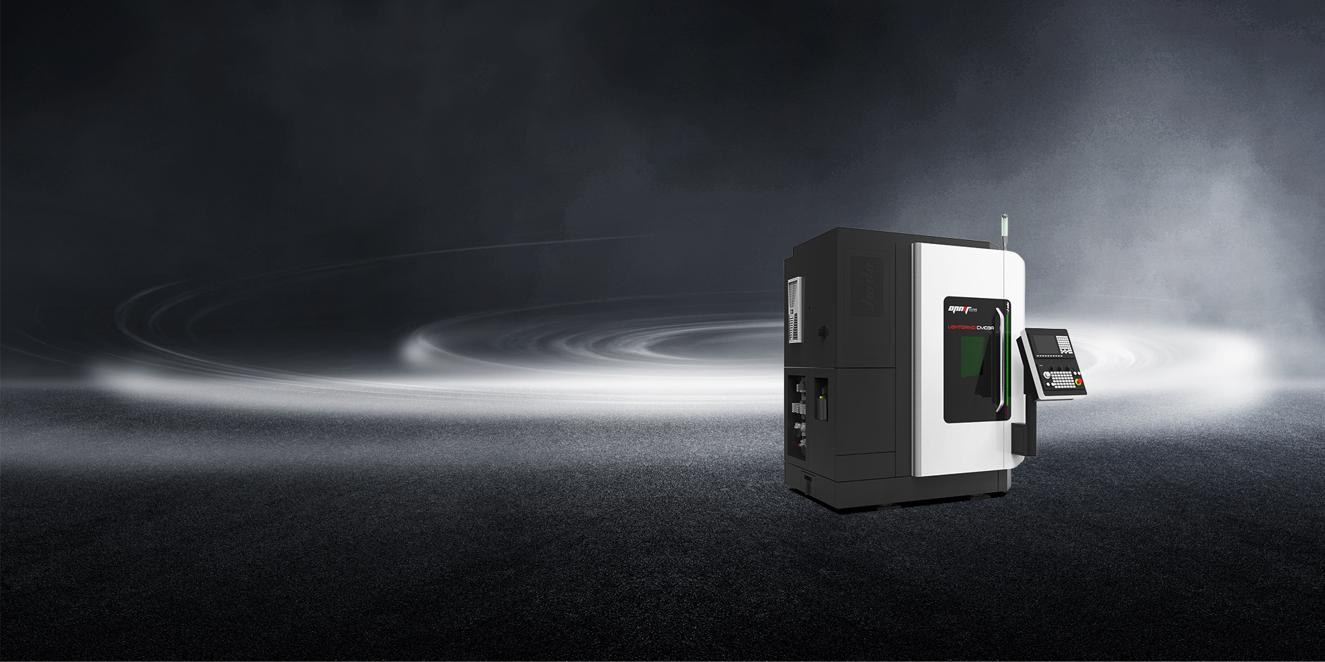
The L320V is OPMT’s workhorse nanosecond platform. Reliable, cost-effective, adequate for non-critical applications.
Laser specifications:
Processing capabilities:
Key features:
Applications:
The Light 5X 40V represents OPMT’s advanced picosecond technology. Higher precision, better surface quality, more flexibility. Costs more but delivers measurably better results.
Nanosecond Q-switched fiber lasers:
Picosecond mode-locked lasers:
The practical limitation is average power. A 50W laser at 1MHz delivers 50μJ per pulse. At 100kHz it’s 500μJ per pulse. Higher energy per pulse means fewer passes needed.
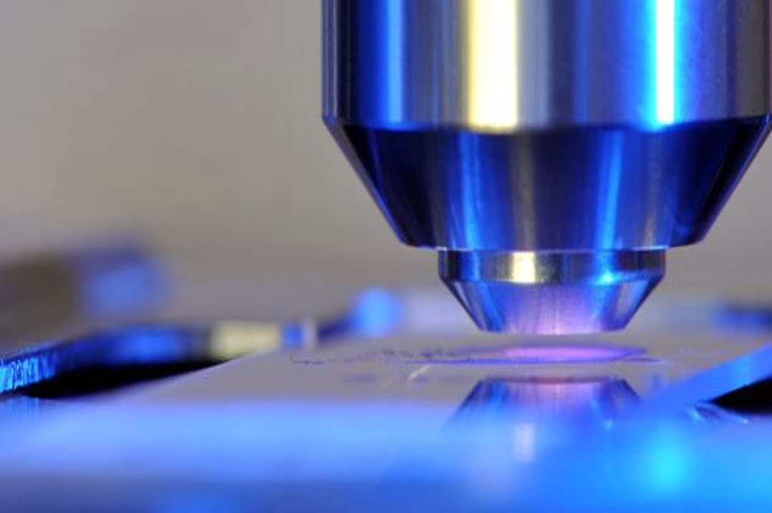
Both systems use galvanometer scanners for beam positioning:
Standard galvo specs:
OPMT modular galvo systems:
The modular design allows swapping different focusing optics (127mm, 160mm, 254mm focal lengths) without realigning the beam path. Setup time drops from 2-3 hours to under 30 minutes.
OPMT’s iMTOS control platform provides:
These features matter for complex 3D geometries. Synchronizing laser firing with 5-axis position to within 10μs prevents errors when machining curved surfaces.
| Parameter | L320V (Nanosecond) | Light 5X 40V (Picosecond) |
|---|---|---|
| Pulse width | 30-500ns | ~10-50ps |
| Average power | 100W | 20-50W |
| Processing speed | 100mm/s | 250mm/s (finishing) |
| HAZ width (steel) | 60-80μm | 15-25μm |
| Surface finish | Ra 0.8-1.5μm | Ra 0.15-0.4μm |
| Positioning accuracy | ±5μm | ±3μm |
| Number of axes | 3 | 5 |
| System price | $285,000 | $450,000 |
The specifications show clear trade-offs. Nanosecond delivers higher average power and lower cost. Picosecond provides better surface quality, smaller HAZ, and more precision.
Choosing between picosecond and nanosecond lasers requires matching technology capabilities to application requirements. Nanosecond systems deliver cost-effective material removal when HAZ above 50μm is acceptable. Picosecond provides superior surface quality and minimal thermal damage for precision applications.
The data from OPMT’s deployed systems quantifies the differences: nanosecond HAZ of 60-80μm vs picosecond 15-25μm on 316L steel, surface finish improving from Ra 1.5μm to Ra 0.3μm, microcrack elimination in 90% of samples. These aren’t small differences.
For production environments processing thousands of parts annually, TCO analysis shows picosecond paying back its premium in 2-5 years through reduced post-processing and improved yield. Lower volume applications struggle to justify the investment.
Industry-specific requirements drive many decisions. Medical device manufacturing defaults to picosecond for regulatory certainty. Automotive tooling uses hybrid processing. Aerospace evaluates case-by-case based on component criticality.
The technical specifications comparison reveals that both technologies have clear roles. OPMT’s L320V nanosecond platform handles bulk material removal and applications with relaxed tolerances. The Light 5X 40V picosecond system delivers precision finishing and minimal HAZ for critical components.
Make your selection based on measured requirements, not marketing claims. Run sample parts, measure HAZ with cross-sectional analysis, verify surface finish with profilometry. The right technology for your application becomes obvious when you test it.
For manufacturers exploring the complete spectrum of ultrafast laser technologies, our comprehensive guide to femtosecond laser applications provides additional context on even shorter pulse durations and their unique advantages for extreme precision applications.
Disclaimer
This content is compiled by OPMT Laser based on publicly available information for reference only; mentions of third-party brands and products are for objective comparison and do not imply any commercial association or endorsement.
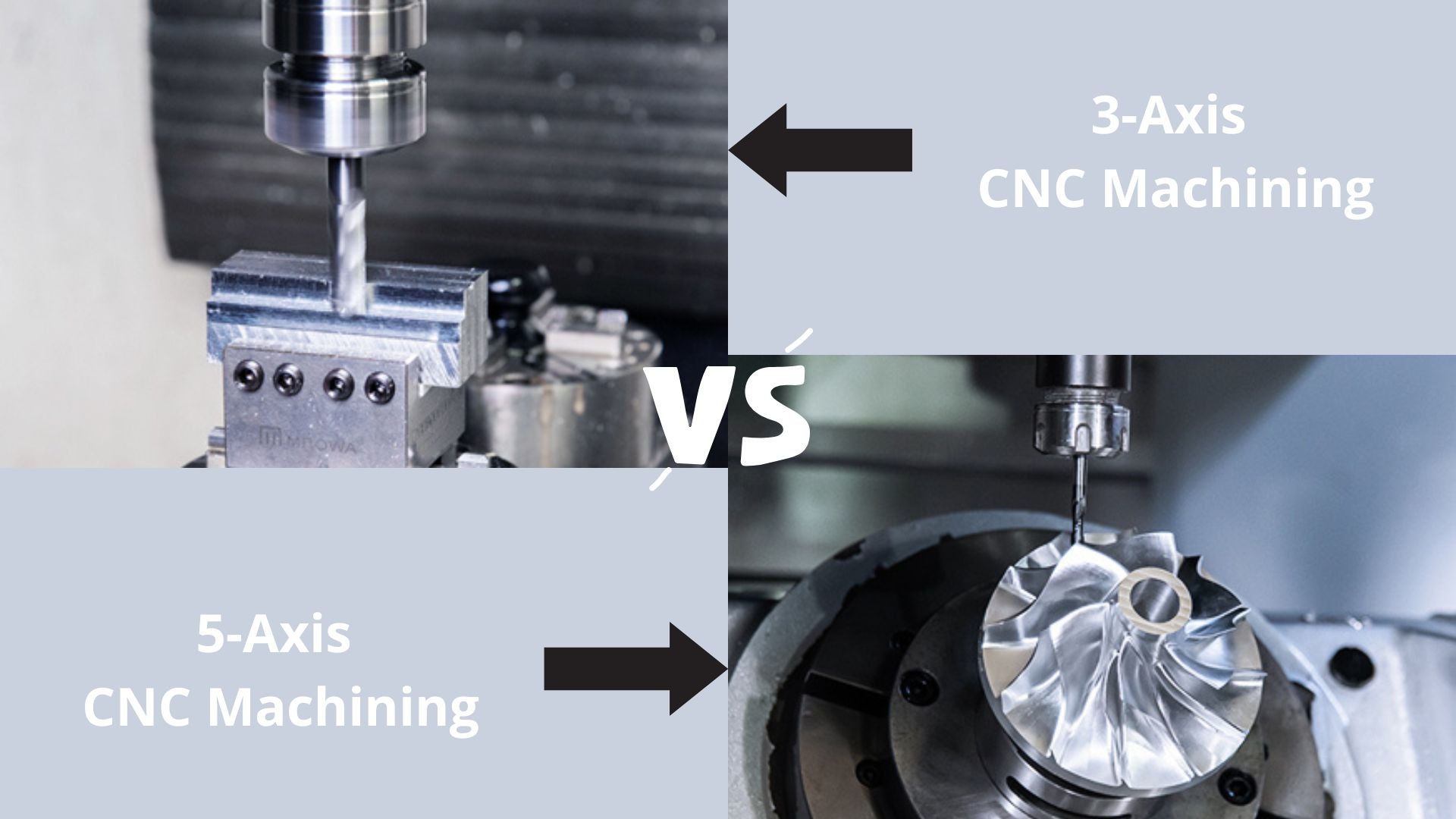
Explore the world of CNC machining as we compare 3-axis and 5-axis technologies. From basic operations to complex geometries, find out which machine suits your manufacturing needs in 2025.
Explore OPMT’s proven 5-phase ODM process for custom laser systems. ISO-certified manufacturing, ±0.003mm precision, IP protection. Submit project requirements today.

Looking for the best 5-axis CNC machining center suppliers? Check our top 10 list for expert insights and find the perfect fit for your needs!
Explore the top 10 laser metal cutting machines of 2025, featuring industry leaders like Trumpf, Bystronic, and OPMT Laser. Compare cutting-edge technology, precision, and efficiency to find the perfect solution for your manufacturing needs.
Please fill in your contact information to download the PDF.