Programar una visita
Independientemente de si necesita asesoramiento general o apoyo específico, estaremos encantados de ayudarle.
Independientemente de si necesita asesoramiento general o apoyo específico, estaremos encantados de ayudarle.
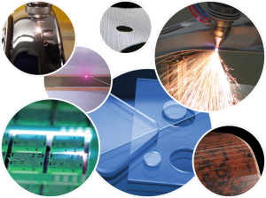
La elección entre láseres de femtosegundos y de nanosegundos para el micromecanizado determina directamente las tolerancias alcanzables, la zona afectada por el calor (ZAT), la integridad superficial y el coste de la calidad a largo plazo en entornos de fabricación regulados. Para los responsables de I+D y los ingenieros de fabricación de precisión, la decisión fundamental radica en si las ventajas de rendimiento, calidad y cumplimiento normativo de la tecnología de femtosegundos justifican la mayor complejidad del sistema en comparación con las plataformas de nanosegundos consolidadas en una aplicación específica de medicina, semiconductores o herramientas.
Para obtener una descripción general básica de los principios y arquitecturas de sistemas de láser ultrarrápido, consulte Tecnología láser femto: corte y procesamiento ultraprecisos.
Tanto los láseres de femtosegundos como los de nanosegundos suministran energía pulsada, pero la duración de sus pulsos difiere en aproximadamente seis órdenes de magnitud: los pulsos de femtosegundos son del orden de 10⁻¹⁵ segundos, mientras que los de nanosegundos rondan los 10⁻⁹ segundos. Esta diferencia temporal modifica fundamentalmente la forma en que la energía láser se acopla al material y la propagación del calor durante el micromaquinado.
En el procesamiento de nanosegundos, el pulso es lo suficientemente largo como para lograr un acoplamiento electrón-fonón significativo y la conducción de calor hacia la red circundante, por lo que la eliminación de material está dominada por efectos fototérmicos como la fusión, la vaporización y la resolidificación. En el procesamiento de femtosegundos, el pulso es más corto que el tiempo característico de difusión térmica, y la transferencia de energía se produce mediante absorción no lineal e ionización ultrarrápida, a menudo descrita como fotodisrupción o «ablación casi fría».
Dado que los pulsos de femtosegundos terminan antes de que la red pueda calentarse significativamente, la energía se confina a un volumen muy pequeño y se expulsa rápidamente, dejando solo una ZAC mínima en la mayoría de los materiales de ingeniería. Por el contrario, los pulsos de nanosegundos permiten que el calor se difunda decenas de micrómetros o más, creando una ZAC visible, capas de refusión y posibles microfisuras alrededor de la estructura, lo cual puede ser aceptable o no según la aplicación.
Los datos experimentales e industriales muestran consistentemente anchos de ZAT de decenas de micrómetros para el micromecanizado de nanosegundos, frente a solo unos pocos micrómetros (o por debajo del límite de detección óptica) para el procesamiento de femtosegundos. OPMT informa valores típicos de ZAT de nanosegundos de 50 a 100 μm en componentes metálicos, mientras que los sistemas de femtosegundos en los mismos materiales los reducen a menos de 5 μm.
Las comparaciones publicadas confirman que los pulsos de nanosegundos pueden producir bandas de ZAT de aproximadamente 40 μm en metales, mientras que los pulsos de femtosegundos, en condiciones de fluencia similares, pueden no producir ZAT observable en la inspección transversal. Esta diferencia es decisiva en aplicaciones donde las restricciones regulatorias o funcionales limitan considerablemente el daño térmico alrededor de una característica cortada o perforada.
El micromecanizado de nanosegundos tiende a mostrar bordes fundidos y resolidificados, rebabas y capas refundidas en los bordes de las características, especialmente en metales y cerámicas frágiles. Estos artefactos térmicos suelen requerir posprocesamiento, como desbarbado mecánico, grabado químico o pulido, lo cual incrementa el coste, aumenta el tiempo de procesamiento y presenta el riesgo de deriva dimensional.
El micromecanizado de femtosegundos, que aprovecha la ablación casi fría, suele producir bordes afilados con rebabas significativamente reducidas y un recasting insignificante, incluso en materiales duros como el diamante, el carburo de silicio y la cerámica avanzada. Los datos de OPMT muestran que las microestructuras procesadas por femtosegundos alcanzan tolerancias dimensionales del orden de ±10 μm con un desprendimiento mínimo de los bordes, en comparación con los resultados de nanosegundos en geometrías similares.
Los láseres de nanosegundos pueden lograr una rugosidad aceptable para muchas piezas industriales, pero la combinación de la dinámica de fusión y las salpicaduras limita su idoneidad para la ingeniería de superficies submicrónicas y las microtexturas funcionales. Además, los ciclos térmicos repetidos pueden inducir microfisuras que comprometen la resistencia a la fatiga en aleaciones de alto rendimiento.
Los sistemas de femtosegundos de OPMT alcanzan valores de rugosidad superficial de aproximadamente 0,08–0,1 μm en componentes de titanio, diamante y cerámica, y mantienen precisiones de posicionamiento de aproximadamente ±0,003 mm en configuraciones de mecanizado de cinco ejes. Esto permite obtener microcaracterísticas de alta fidelidad, texturizado superficial funcional, como las estructuras superficiales periódicas inducidas por láser (LIPSS), y un rendimiento constante en aplicaciones médicas y de semiconductores exigentes.
La forma más eficaz de evaluar los láseres de femtosegundos frente a los de nanosegundos es considerar las clases de aplicación específicas y sus requisitos de calidad y cumplimiento.
Para una comparación más amplia de los regímenes de pulsos en entornos CNC, consulte Láseres de nanosegundos, picosegundos y femtosegundos para CNC.
En la fabricación de stents cardiovasculares, el procesamiento láser debe controlar la ZAT para evitar alteraciones en la microestructura de la aleación, la integridad del recubrimiento o la geometría del lumen que puedan influir en el riesgo de reestenosis y trombosis. Los sistemas láser ultrarrápidos con una ZAT estrictamente controlada y superficies de struts lisas se asocian con un mejor rendimiento clínico en diseños avanzados de stents y respaldan una rigurosa validación de dispositivos.

Los sistemas de femtosegundos son especialmente adecuados para:
Los láseres de nanosegundos aún pueden servir para geometrías de stents o implantes más simples donde una zona afectada por el calor ligeramente más grande y bordes más rugosos siguen siendo clínicamente aceptables, especialmente si ya se cuenta con procesos de limpieza validados y un acabado secundario robusto.
En el caso de obleas semiconductoras y sustratos cerámicos, las microfisuras, el astillamiento y los daños subsuperficiales afectan directamente el rendimiento, el rendimiento paramétrico y la fiabilidad a largo plazo. Los procesos basados en nanosegundos pueden alcanzar niveles de defectos aceptables para algunos sustratos robustos, pero el astillamiento y el agrietamiento térmico pueden resultar limitantes a medida que disminuye el espesor de la oblea o se reducen las normas de diseño.
El micromecanizado de femtosegundos permite el taladrado y corte de precisión de materiales como carburo de silicio, diamante CVD y cerámicas avanzadas, con un daño mínimo alrededor de las vías y las líneas de corte. OPMT informa que las configuraciones ultrarrápidas e híbridas reducen significativamente los defectos de las obleas en entornos de producción de alto volumen, mejorando así el rendimiento efectivo a nivel de línea al incluir los desechos y el reprocesamiento en el cálculo.
En el vidrio de vitrina y de cubierta, la calidad del borde de corte determina la resistencia a la flexión, el rendimiento óptico y el rendimiento de la laminación posterior. Los láseres de nanosegundos tienden a generar microfisuras y astillas debido a la tensión térmica y la expansión diferencial, lo que obliga a utilizar ventanas de proceso conservadoras y a un posprocesamiento considerable.
Los láseres ultrarrápidos, incluidos los sistemas de femtosegundos, pueden producir bordes más lisos y con mínimas grietas, y permiten geometrías innovadoras, como muescas o características internas en vidrio delgado para pantallas plegables. Los datos del caso OPMT destacan que un mejor control de la ZAT y la integridad de los bordes contribuyen directamente a una mayor eficiencia y rendimiento en las líneas de producción de OLED y pantallas flexibles.
Los láseres de nanosegundos se utilizan ampliamente para texturizado robusto de moldes y grabado de uso general, donde las microfisuras y la ZAT son manejables o incluso beneficiosas para la adhesión mecánica. Ofrecen una integración relativamente sencilla y un procesamiento rentable para texturas más grandes y superficies menos críticas.
Los sistemas de femtosegundos destacan en el texturizado de moldes de alta gama y el micromecanizado de materiales superduros, incluyendo geometría de herramientas de diamante, insertos de molde microestructurados y texturas 3D de forma libre. Las plataformas de femtosegundos de cinco ejes de OPMT admiten tamaños de punto ultrapequeños y texturas multicapa, lo que permite obtener micro-nanoestructuras con rugosidad submicrónica en superficies 3D complejas.
Para obtener información detallada sobre el micromaquinado de diamantes con láseres de femtosegundos, consulte Micromecanizado de diamante con láser de femtosegundos.
| Criterio / Aplicación | Resultado típico del láser de nanosegundos | Resultado típico del láser de femtosegundo |
|---|---|---|
| ZAT en metales | ~50–100 μm HAZ, refundición visible y tintado térmico | <5 μm HAZ, a menudo por debajo de la detección óptica |
| Corte de stents médicos | Aceptable para diseños básicos con posprocesamiento. | Permite puntales finos, lúmenes suaves y daño mínimo al revestimiento. |
| Perforación/trazado de obleas de semiconductores | Riesgo de microfisuras y astillas en obleas frágiles | Daños mínimos en el subsuelo, mayor rendimiento en materiales frágiles |
| Corte de vidrio para pantallas OLED | Microfisuras en los bordes, mayor riesgo de rotura | Bordes lisos, resistencia a la flexión y rendimiento mejorados. |
| Texturizado de moldes y grabado general | Rentable para texturas no críticas | Microtexturas de alta fidelidad con rugosidad submicrónica |
| Herramientas superduras/de diamante | Daño térmico, probable microfisuras. | Ablación casi en frío, estructura cristalina preservada |
Los láseres de nanosegundos suelen asociarse con altas velocidades de corte lineal en metales convencionales y geometrías relativamente simples. En muchas configuraciones industriales, pueden ofrecer velocidades de línea adecuadas para la producción en grandes lotes de piezas de exigencia moderada, especialmente cuando se aceptan zonas térmicas (ZAT) moderadas y rutas de posprocesamiento conocidas.
Los sistemas de femtosegundos pueden alcanzar velocidades de escaneo y corte altamente competitivas en microcaracterísticas, ya que cada pulso elimina el material eficientemente y requiere un tiempo de recuperación mínimo entre pasadas. Los datos comparativos de OPMT indican que los sistemas ultrarrápidos pueden alcanzar un mayor rendimiento efectivo en microcaracterísticas complejas al reducir o eliminar el acabado secundario y las tasas de rechazo.
Si bien el costo de capital de la tecnología de femtosegundos es mayor, las líneas basadas en nanosegundos pueden generar costos ocultos por desechos, retrabajo y menor rendimiento del dispositivo en aplicaciones sensibles. En implantes y stents médicos, un mejor acabado superficial y una menor ZAT gracias a los láseres ultrarrápidos se han correlacionado con mejores resultados clínicos y menos complicaciones postoperatorias en programas de dispositivos documentados.
En la industria aeroespacial y en componentes mecánicos de alto rendimiento, las superficies procesadas por femtosegundos con muy baja rugosidad y mínima microfisura pueden mejorar significativamente la resistencia a la fatiga y la fiabilidad. OPMT informa que el procesamiento ultrarrápido del titanio y otras aleaciones de alto rendimiento se ha asociado con mejoras mensurables en el rendimiento a la fatiga, en comparación con las superficies afectadas térmicamente.
La inversión en femtosegundos suele justificarse cuando:
Cuando los requisitos funcionales y regulatorios son más flexibles y el posprocesamiento simple es aceptable y ya está validado, los sistemas de nanosegundos pueden seguir siendo la opción más rentable.
Un marco de decisión práctico puede basarse en tres ejes: tolerancia dimensional, ZAT aceptable y sensibilidad del material.
Las clases de materiales que favorecen fuertemente el micromaquinado de femtosegundos incluyen aleaciones biocompatibles para implantes, cerámicas y vidrios frágiles, sustratos semiconductores y materiales superduros como el diamante.
La tecnología de nanosegundos generalmente es adecuada cuando:
Los ejemplos incluyen codificación QR y marcado en instrumentos médicos, corte de metal en general donde la ZAT no es crítica y muchas tareas de grabado y marcado industriales.
Los sistemas de femtosegundos son la opción preferida cuando:
En tales proyectos, el costo incremental del equipo generalmente se compensa con una menor cantidad de desechos, menos pasos de procesamiento y un rendimiento superior del producto final durante la vida útil del programa.
Dado que cada proyecto presenta geometrías, pilas de materiales y requisitos de rendimiento únicos, los responsables de I+D y los ingenieros de procesos suelen validar los procesos candidatos mediante pruebas de muestra en piezas y materiales reales. La realización de ensayos comparativos en plataformas de nanosegundos y femtosegundos con configuraciones de producción proporciona datos concretos sobre la ZAT, la rugosidad, el tiempo de ciclo y el coste unitario, que pueden vincularse directamente con los CTQ internos y las restricciones regulatorias.
OPMT ofrece procesamiento de muestras centrado en aplicaciones para ayudar a cuantificar estas compensaciones, lo que permite a los equipos crear casos de negocios internos para cualquiera de las tecnologías basándose en resultados medidos en lugar de suposiciones.
Los centros de mecanizado CNC de femtosegundos de OPMT combinan una duración de pulso inferior a 400 fs con cinemática multieje, lo que proporciona una precisión de posicionamiento del orden de ±0,003 mm y una repetibilidad cercana a ±0,002 mm para estructuras 3D complejas. Estas plataformas están diseñadas para aplicaciones de alta precisión, como el micromecanizado con herramientas de diamante, moldes microtexturizados y componentes médicos o semiconductores avanzados, donde la ZAT y las microfisuras deben controlarse rigurosamente.
Para conocer las especificaciones y capacidades concretas a nivel de máquina, consulte Centro de mecanizado láser de femtosegundos de cinco ejes Micro3D L530V.
La óptica estrechamente integrada, las estructuras de máquina de alta estabilidad y el control inteligente del movimiento permiten tamaños de punto focal muy pequeños y ventanas de proceso estables, lo que permite obtener microcaracterísticas con tolerancias dimensionales de alrededor de ±10 μm y rugosidad superficial inferior a 1 μm, incluso en materiales complejos. Combinados con la monitorización de procesos y bibliotecas de parámetros conformes a las prácticas de la norma ISO 9001, estos sistemas facilitan la producción estable y escalable de microestructuras y nanoestructuras a gran escala.
OPMT también suministra sistemas láser CNC basados en nanosegundos que priorizan el rendimiento y la rentabilidad en aplicaciones donde se aceptan condiciones de zona afectada por el calor (ZAC) moderadas y posprocesamiento. Estas plataformas son ideales para marcado, corte general y diversas características estructurales en la fabricación automotriz, aeroespacial e industrial en general, donde los requisitos de calidad de los bordes son menos estrictos.
Al aprovechar las tecnologías de nanosegundos establecidas con sistemas de movimiento robustos y recetas de procesos comprobadas, los fabricantes pueden lograr costos por pieza atractivos y, al mismo tiempo, mantener una calidad de borde suficiente y un control dimensional para aplicaciones menos sensibles.
Para las organizaciones que deciden entre el micromecanizado láser de femtosegundos y nanosegundos, una prueba de procesamiento de muestras específica para cada aplicación es la vía más directa para tomar una decisión segura y basada en la evidencia. OPMT puede procesar sus materiales y geometrías reales con ambas tecnologías, documentar la ZAT, la rugosidad superficial, la precisión dimensional y los tiempos de ciclo, y ayudar a cuantificar el retorno de la inversión (ROI) y el perfil de riesgo de cada enfoque.
Para iniciar una evaluación específica del proyecto, los equipos de I+D y de procesos pueden solicitar una prueba de procesamiento de muestra y compartir dibujos, tolerancias, pilas de materiales y requisitos de cumplimiento para que Los ingenieros de OPMT puede proponer una ventana de proceso optimizada alineada con la norma ISO 9001 y las necesidades de validación específicas del sector.
Los láseres de femtosegundos funcionan con duraciones de pulso de alrededor de 10⁻¹⁵ s, lo que permite una ablación casi en frío y una ZAT muy pequeña, mientras que los láseres de nanosegundos utilizan pulsos de 10⁻⁹ s y se basan principalmente en la eliminación de material térmico, lo que genera una ZAT más grande y más refundición.
El procesamiento de femtosegundos reduce drásticamente la ZAT (a menudo por debajo de los 5 μm y a veces por debajo del nivel de detección en ciertos materiales), pero no todas las configuraciones producen una influencia térmica literalmente cero; los parámetros del proceso y las propiedades del material aún juegan un papel.
Los láseres de nanosegundos son suficientes cuando las tolerancias son del orden de decenas de micrómetros, una HAZ moderada es aceptable y un posprocesamiento simple puede gestionar la calidad del borde; se utilizan comúnmente para metales robustos, marcados y microcaracterísticas menos críticas.
Para diseños de stents avanzados, los láseres de femtosegundos y otros láseres ultrarrápidos ofrecen un control superior sobre la zona afectada por el calor (HAZ), la suavidad del lumen y la integridad del recubrimiento, lo que favorece un mejor rendimiento clínico, mientras que los sistemas de nanosegundos aún se pueden utilizar en aplicaciones de stents más simples o menos exigentes.
Los láseres ultrarrápidos, incluidos los sistemas de femtosegundos, pueden reducir significativamente las microfisuras y astillas en los bordes del vidrio, mejorando la resistencia a la flexión y el rendimiento de línea en la fabricación de pantallas, lo que es particularmente importante para sustratos de vidrio delgados y plegables.
Aunque los equipos de femtosegundos son más complejos, el rendimiento efectivo en microcaracterísticas complejas puede ser mayor porque dichos sistemas requieren menos pasadas, un posprocesamiento mínimo y producen menos rechazos, mientras que los sistemas de nanosegundos aún pueden ofrecer el menor costo por pieza para características simples y tolerantes.
OPMT ofrece plataformas CNC de nanosegundos y femtosegundos y ofrece servicios de procesamiento de muestras para comparar la calidad, la zona afectada por el calor (HAZ) y los tiempos de ciclo en piezas reales, brindando a los equipos de ingeniería información basada en datos para decisiones de selección de procesos y CAPEX.
Descargo de responsabilidad
Este contenido es compilado por OPMT Laser con base en información pública disponible únicamente como referencia; las menciones de marcas y productos de terceros son para comparación objetiva y no implican ninguna asociación o respaldo comercial.
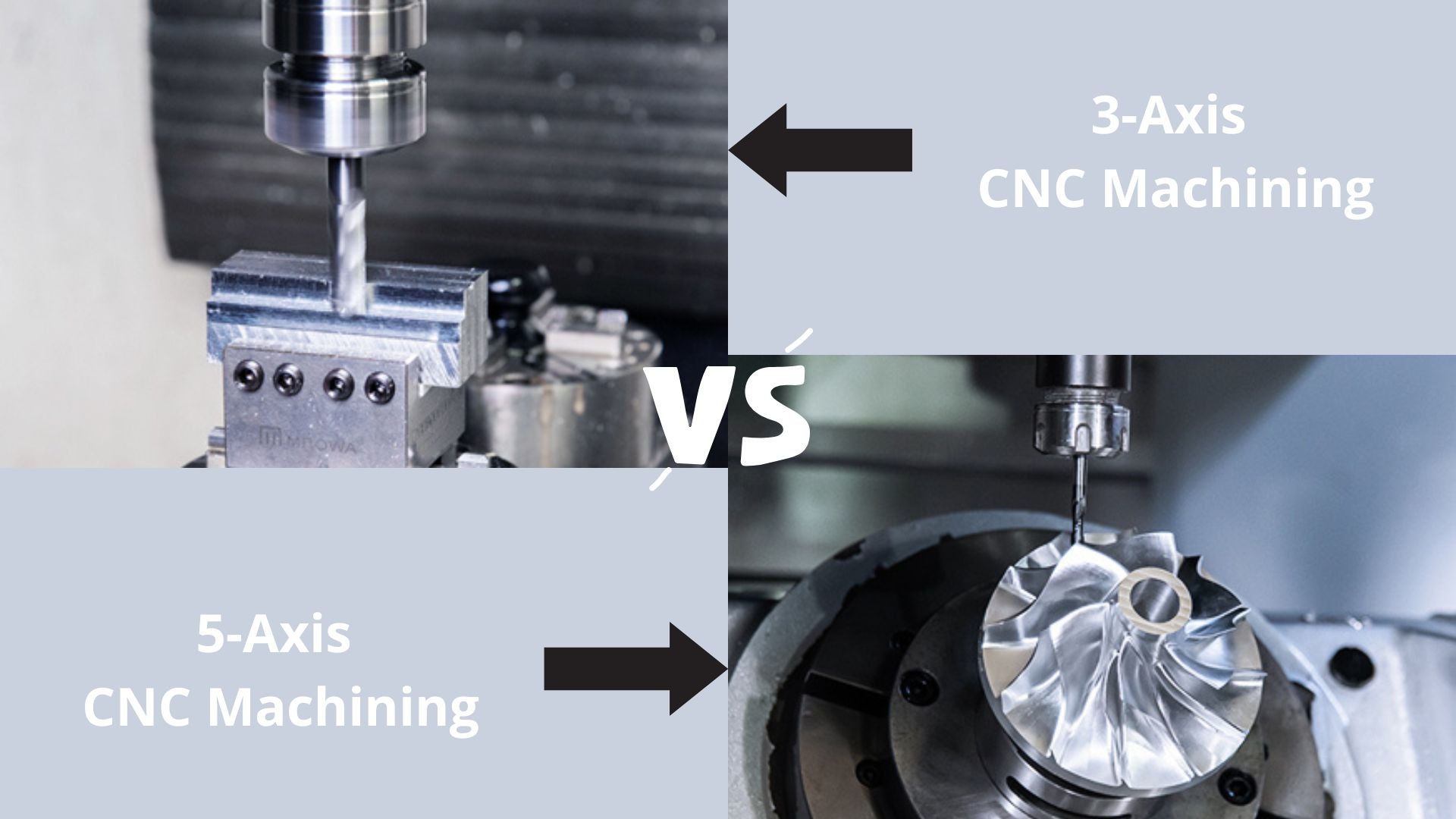
Explore el mundo del mecanizado CNC mientras comparamos las tecnologías de 3 y 5 ejes. Desde operaciones básicas hasta geometrías complejas, descubra qué máquina se adapta a sus necesidades de fabricación en 2025.
Explore el probado proceso ODM de 5 fases de OPMT para sistemas láser personalizados. Fabricación con certificación ISO, precisión de ±0,003 mm y protección IP. Envíe los requisitos de su proyecto hoy mismo.
¿Está buscando los mejores proveedores de centros de mecanizado CNC de 5 ejes? ¡Consulte nuestra lista de los 10 mejores para obtener información de expertos y encontrar el que mejor se adapte a sus necesidades!
Explore las 10 mejores máquinas de corte de metales por láser de 2025, con líderes de la industria como Trumpf, Bystronic y OPMT Laser. Compare la tecnología de vanguardia, la precisión y la eficiencia para encontrar la solución perfecta para sus necesidades de fabricación.
Por favor, rellene sus datos de contacto para descargar el PDF.