Schedule a Visit
Regardless of whether you require general advice or specific support, we are happy to help you.
Regardless of whether you require general advice or specific support, we are happy to help you.
Choosing between femtosecond and nanosecond lasers for micromachining directly determines achievable tolerances, heat-affected zone (HAZ), surface integrity, and long-term cost of quality in regulated manufacturing environments. For R&D managers and precision manufacturing engineers, the core decision is whether the performance, quality, and compliance advantages of femtosecond technology justify the higher system complexity compared with mature nanosecond platforms in a specific medical, semiconductor, or tooling application.
For a foundational overview of ultrafast laser principles and system architectures, see Femto Laser Technology: Ultra-Precise Cutting & Processing.
Femtosecond and nanosecond lasers both deliver pulsed energy, but their pulse durations differ by roughly six orders of magnitude: femtosecond pulses are on the order of 10⁻¹⁵ seconds, while nanosecond pulses are around 10⁻⁹ seconds. This timescale difference fundamentally changes how laser energy couples into the material and how heat propagates during micromachining.

In nanosecond processing, the pulse is long enough for significant electron–phonon coupling and heat conduction into the surrounding lattice, so material removal is dominated by photothermal effects such as melting, vaporization, and resolidification. In femtosecond processing, the pulse is shorter than the characteristic thermal diffusion time, and energy transfer proceeds via nonlinear absorption and ultrafast ionization, often described as photodisruption or “near cold ablation.”
Because femtosecond pulses end before the lattice can heat significantly, energy is confined to a very small volume and ejected rapidly, leaving only a minimal HAZ in most engineering materials. By contrast, nanosecond pulses allow heat to diffuse tens of micrometers or more, creating a visible HAZ, recast layers, and possible micro-cracks around the feature, which may or may not be acceptable depending on the application.
Experimental and industrial data consistently show HAZ widths in the tens of micrometers for nanosecond micromachining, versus only a few micrometers—or below the optical detection limit—for femtosecond processing. OPMT reports typical nanosecond HAZ values of 50–100 μm in metallic components, while femtosecond systems in the same materials reduce this to below 5 μm.
Published comparisons confirm that nanosecond pulses can produce HAZ bands of roughly 40 μm in metals, whereas femtosecond pulses under similar fluence conditions may yield no observable HAZ in cross-sectional inspection. This difference is decisive in applications where regulatory or functional constraints tightly limit thermal damage around a cut or drilled feature.
Nanosecond micromachining tends to show melted and resolidified rims, burrs, and recast layers on feature edges, particularly in metals and brittle ceramics. These thermal artifacts often require post-processing such as mechanical deburring, chemical etching, or polishing, all of which add cost, increase takt time, and introduce the risk of dimensional drift.
Femtosecond micromachining, leveraging near cold ablation, typically yields sharp edges with significantly reduced burrs and negligible recast, even in hard materials like diamond, silicon carbide, and advanced ceramics. OPMT data show femtosecond-processed microstructures achieving dimensional tolerances on the order of ±10 μm with minimal edge chipping compared to nanosecond results in similar geometries.
Nanosecond lasers can achieve acceptable roughness for many industrial parts, but the combination of melt dynamics and spatter limits their suitability for sub-micron surface engineering and functional micro-textures. In addition, repeated thermal cycling can induce micro-cracks that compromise fatigue life in high-performance alloys.
Femtosecond systems from OPMT reach surface roughness values down to roughly 0.08–0.1 μm on titanium, diamond, and ceramic components and maintain positioning accuracies around ±0.003 mm in five-axis machining configurations. This enables high-fidelity micro-features, functional surface texturing such as laser-induced periodic surface structures (LIPSS), and consistent performance in demanding medical and semiconductor applications.
The most effective way to evaluate femtosecond vs. nanosecond lasers is to consider specific application classes and their quality and compliance requirements.
For a broader comparison of pulse regimes in CNC environments, see Nanosecond vs Picosecond vs Femtosecond Lasers for CNC.
In cardiovascular stent manufacturing, laser processing must control HAZ to avoid altering alloy microstructure, coating integrity, or lumen geometry that can influence restenosis and thrombosis risk. Ultrafast laser systems with tightly controlled HAZ and smooth strut surfaces are associated with improved clinical performance in advanced stent designs and support stringent device validation.

Femtosecond systems are particularly suited to:
Nanosecond lasers can still serve simpler stent or implant geometries where slightly larger HAZ and rougher edges remain clinically acceptable, especially if robust secondary finishing and validated cleaning processes are already in place.
For semiconductor wafers and ceramic substrates, micro-cracking, chipping, and subsurface damage directly impact yield, parametric performance, and long-term reliability. Nanosecond-based processes may reach acceptable defect levels for some robust substrates, but thermal cracking and chipping can become limiting as wafer thickness decreases or as design rules shrink.
Femtosecond micromachining allows precision drilling and cutting of materials like silicon carbide, CVD diamond, and advanced ceramics with minimal damage around vias and scribe lines. OPMT reports that ultrafast and hybrid configurations significantly reduce wafer defects in high-volume production environments, improving effective throughput at the line level when scrap and rework are included in the calculation.
In display and cover glass, the quality of the cut edge drives bending strength, optical performance, and downstream lamination yields. Nanosecond lasers tend to generate micro-cracks and chips due to thermal stress and differential expansion, forcing conservative process windows and substantial post-processing.
Ultrafast lasers, including femtosecond systems, can produce smoother, crack-minimized edges and enable innovative geometries such as notches or internal features in thin glass for foldable displays. OPMT case data highlight that improved HAZ control and edge integrity directly contribute to higher efficiency and yield in OLED and flexible-display production lines.
Nanosecond lasers are widely used for robust mold texturing and general-purpose engraving where micro-cracks and HAZ are manageable or even beneficial for mechanical adhesion. They offer comparatively simple integration and cost-effective processing for larger textures and less critical surfaces.
Femtosecond systems excel in high-end mold texturing and superhard-material micromachining, including diamond tool geometry, micro-structured mold inserts, and freeform 3D textures. OPMT’s five-axis femtosecond platforms support ultra-small spot sizes and multi-layer textures, enabling micro-nano structures with sub-micron roughness on complex 3D surfaces.
For detailed insights into diamond micromachining with femtosecond lasers, see Femtosecond Laser Diamond Micromachining.
| Criterion / Application | Nanosecond Laser Typical Outcome | Femtosecond Laser Typical Outcome |
|---|---|---|
| HAZ in metals | ~50–100 μm HAZ, visible recast and thermal tinting | <5 μm HAZ, often below optical detection |
| Medical stent cutting | Acceptable for basic designs with post-processing | Enables fine struts, smooth lumens, minimal coating damage |
| Semiconductor wafer drilling/scribing | Risk of micro-cracks and chips in brittle wafers | Minimal subsurface damage, higher yield on brittle materials |
| OLED/display glass cutting | Edge micro-cracks, higher breakage risk | Smooth edges, improved bending strength and yield |
| Mold texturing & general engraving | Cost-effective for non-critical textures | High-fidelity micro-textures with sub-micron roughness |
| Superhard / diamond tools | Thermal damage, micro-cracking likely | Near cold ablation, preserved crystalline structure |
Nanosecond lasers are often associated with high linear cutting speeds in conventional metals and relatively simple geometries. In many industrial configurations, they can deliver line speeds suitable for large-batch production of moderately demanding parts, particularly when modest HAZ and known post-processing routes are acceptable.
Femtosecond systems can achieve highly competitive scanning and cutting speeds in micro-scale features because each pulse removes material efficiently and requires minimal recovery time between passes. OPMT comparative data indicate that ultrafast systems can reach higher effective throughput on complex micro-features by reducing or eliminating secondary finishing and lowering reject rates.
While the capital cost of femtosecond technology is higher, nanosecond-based lines may incur hidden costs through scrap, rework, and reduced device performance in sensitive applications. In medical implants and stents, improved surface finish and reduced HAZ from ultrafast lasers have been correlated with better clinical outcomes and fewer postoperative complications in documented device programs.
In aerospace and high-performance mechanical components, femtosecond-processed surfaces with very low roughness and minimal micro-cracking can significantly improve fatigue life and reliability. OPMT reports that ultrafast processing of titanium and other high-performance alloys has been associated with measurable gains in fatigue performance compared with thermally affected surfaces.
The femtosecond investment is most often justified when:
Where functional and regulatory requirements are more forgiving, and simple post-processing is acceptable and already validated, nanosecond systems can remain the more cost-effective choice.
A practical decision framework can be based on three axes: dimensional tolerance, acceptable HAZ, and material sensitivity.
Material classes that strongly favor femtosecond micromachining include biocompatible alloys for implants, brittle ceramics and glasses, semiconductor substrates, and superhard materials such as diamond.
Nanosecond technology is generally suitable when:
Examples include QR coding and marking on medical instruments, general metal cutting where HAZ is not critical, and many industrial engraving and marking tasks.
Femtosecond systems are the preferred choice when:
In such projects, the incremental equipment cost is typically offset by reduced scrap, fewer processing steps, and superior end-product performance over the program’s lifetime.
Because each project has unique geometries, material stacks, and performance requirements, R&D managers and process engineers usually validate candidate processes via sample testing on real parts and materials. Running comparative trials on nanosecond and femtosecond platforms with production-grade setups provides concrete data on HAZ, roughness, cycle time, and cost per unit that can be tied directly to internal CTQs and regulatory constraints.
OPMT offers application-focused sample processing to help quantify these trade-offs, enabling teams to build internal business cases for either technology based on measured outcomes rather than assumptions.
OPMT’s femtosecond CNC machining centers combine sub-400 fs pulse duration with multi-axis kinematics, delivering positioning accuracy on the order of ±0.003 mm and repeatability near ±0.002 mm for complex 3D structures. These platforms are designed for high-precision applications such as diamond tool micromachining, micro-textured molds, and advanced medical or semiconductor components where HAZ and micro-cracking must be tightly controlled.
For concrete machine-level specifications and capabilities, see Micro3D L530V Five-Axis Femtosecond Laser Machining Center.
Tightly integrated optics, high-stability machine structures, and intelligent motion control allow very small focused spot sizes and stable process windows, enabling micro-features with dimensional tolerances around ±10 μm and surface roughness below 1 μm, even on challenging materials. Combined with process monitoring and parameter libraries aligned to ISO 9001 practices, these systems support stable, scalable production of micro-nano structures at industrial volumes.
OPMT also supplies nanosecond-based CNC laser systems that prioritize throughput and cost-efficiency in applications where moderate HAZ and post-processing are acceptable. These platforms are well-suited to marking, general cutting, and many structural features in automotive, aerospace, and general industrial manufacturing where edge quality requirements are less stringent.
By leveraging established nanosecond technologies with robust motion systems and proven process recipes, manufacturers can achieve attractive cost per part while maintaining sufficient edge quality and dimensional control for less sensitive applications.
For organizations deciding between femtosecond and nanosecond laser micromachining, an application-specific sample processing test is the most direct route to a confident, evidence-based decision. OPMT can process your actual materials and geometries on both technologies, document HAZ, surface roughness, dimensional accuracy, and cycle times, and help quantify the ROI and risk profile of each approach.
To initiate a project-specific evaluation, R&D and process teams can request a sample processing test and share drawings, tolerances, material stacks, and compliance requirements so that OPMT’s engineers can propose an optimized process window aligned with ISO 9001 and sector-specific validation needs.
Femtosecond lasers operate with pulse durations around 10⁻¹⁵ s, enabling near cold ablation and very small HAZ, while nanosecond lasers use 10⁻⁹ s pulses and primarily rely on thermal material removal, leading to larger HAZ and more recast.
Femtosecond processing dramatically reduces HAZ—often to below 5 μm and sometimes below detection in certain materials—but not every configuration yields literally zero thermal influence; process parameters and material properties still play a role.
Nanosecond lasers are sufficient when tolerances are on the order of tens of micrometers, moderate HAZ is acceptable, and simple post-processing can manage edge quality; they are commonly used for robust metals, markings, and less critical micro-features.
For advanced stent designs, femtosecond and other ultrafast lasers offer superior control over HAZ, lumen smoothness, and coating integrity, supporting better clinical performance, while nanosecond systems may still be used in simpler or less demanding stent applications.
Ultrafast lasers, including femtosecond systems, can significantly reduce micro-cracks and chips at glass edges, improving bending strength and line yield in display manufacturing, which is particularly important for thin and foldable glass substrates.
Although femtosecond equipment is more complex, effective throughput on complex micro-features can be higher because such systems require fewer passes, minimal post-processing, and produce fewer rejects, while nanosecond systems may still offer the lowest cost per part for simple, forgiving features.
OPMT provides both nanosecond and femtosecond CNC platforms and offers sample processing services to benchmark quality, HAZ, and cycle times on actual parts, giving engineering teams data-driven input for CAPEX and process selection decisions.
Disclaimer
This content is compiled by OPMT Laser based on publicly available information for reference only; mentions of third-party brands and products are for objective comparison and do not imply any commercial association or endorsement.
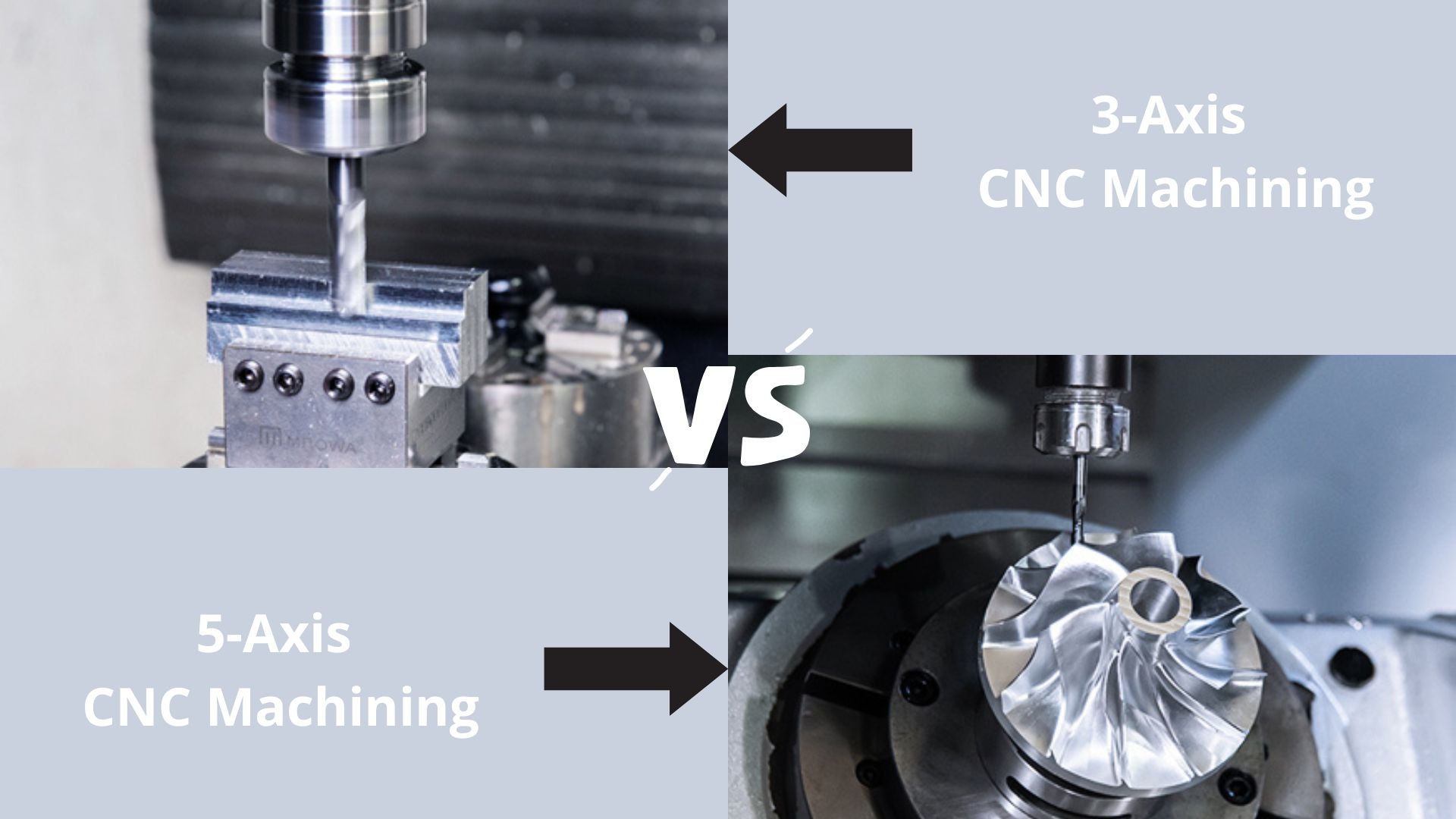
Explore the world of CNC machining as we compare 3-axis and 5-axis technologies. From basic operations to complex geometries, find out which machine suits your manufacturing needs in 2025.
Explore OPMT’s proven 5-phase ODM process for custom laser systems. ISO-certified manufacturing, ±0.003mm precision, IP protection. Submit project requirements today.
Looking for the best 5-axis CNC machining center suppliers? Check our top 10 list for expert insights and find the perfect fit for your needs!
Explore the top 10 laser metal cutting machines of 2025, featuring industry leaders like Trumpf, Bystronic, and OPMT Laser. Compare cutting-edge technology, precision, and efficiency to find the perfect solution for your manufacturing needs.
Please fill in your contact information to download the PDF.